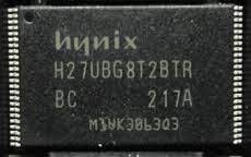
SK hynix H27UBG8T2BTR( BC 612F) 32GB MEMORY IC TSOP-48
F26 32Gb MLC NAND Flash Memory TSOP Legacy
Product Feature
■ Multi Level Cell(MLC) Technology
■ NAND Interface
- x8 bus width
- Multiplexed address/ Data
- Pin-out compatibility for all densities
■ Power Supply Voltage
- VCC = 2.7 V ~ 3.6 V
- VCCQ = 2.7 V ~ 3.6 V / 1.7 V ~ 1.95 V
■ Organization
- Page size : (8K+640spare)bytes - Block size : (2048K+160K)bytes - Plane size : 1024blocks
- Device size : 2048blocks
■ Page Read/Program Time
- Random Read Time(tR): 90us(MLC), 40us(SLC) - Sequential Access: 20 ns (min.)
- Page Program Time: 1300us(MLC), 500us(SLC) - Parallel operations on both planes available, effectively halving program, read and erase time
■ Block Erase
-Block Erase Time: 3.5ms(Typ.)
■ Multi-Plane Architecture
- Two independent planes architecture
- Parallel operations on both planes available, effectively halving program, read and erase time
■ Command Set
- ONFI 2.2 Compliant Command Set - Interleaved Copyback Program
- Read Unique IDs
■ Package
- Package type : TSOP
- Chip count : SDP(1CE, Single) = 1stack
DDP(2CE, Dual) = 2stack - Pin Count : 48
- Size : 12mm x 20mm x 1.2mm
■ Electronic Signature
- 1st cycle: Manufacturer Code
- 2nd cycle: Device Code
- 3rd cycle: Internal chip number, Cell Type, Number of Simultaneously Programmed Pages.
- 4th cycle: Page size, Block size, Organization, Spare size
- 5th cycle: Multi-plane information
- 6th cycle: Technology, EDO, Interface
■ Chip Enable Don’t Care
- Simple interface with microcontroller
■ Hardware Data Protection
- Program/Erase locked during Power transitions

